Electronic color code
The
electronic color code is used to indicate the values or ratings of electronic components, very commonly for resistors, but also for capacitors, inductors, and others. A separate code, the 25-pair color code, is used to identify wires in some telecommunications cables.
The electronic color code was developed in the early 1920s by the Radio Manufacturers Association (now part of Electronic Industries Alliance
(EIA)), and was published as EIA-RS-279. The current international standard is IEC 60062
Colorbands were commonly used (especially on resistors)
because they were easily printed on tiny components, decreasing
construction costs. However, there were drawbacks, especially for color blind
people. Overheating of a component, or dirt accumulation, may make it
impossible to distinguish brown from red from orange. Advances in
printing technology have made printed numbers practical for small
components, which are often found in modern electronics.
Resistor color-coding

One decade of the E12 series (there are twelve preferred values per decade of values) shown with their electronic color codes on resistors.

A 100 kΩ, 5% through-hole resistor.

A 0Ω resistor, marked with a single black band.


A 2260 ohm, 1% precision resistor with 5 color bands (E96 series), from
top 2-2-6-1-1; the last two brown bands indicate the multiplier (x10),
and the 1% tolerance. The larger gap before the tolerance band is
somewhat difficult to distinguish.
To distinguish left from right there is a gap between the C and D bands.
- band A is first significant figure of component value (left side)
- band B is the second significant figure (Some precision resistors have a third significant figure, and thus five bands.)
- band C is the decimal multiplier
- band D if present, indicates tolerance of value in percent (no band means 20%)
For example, a resistor with bands of
yellow, violet, red, and gold
will have first digit 4 (yellow in table below), second digit 7
(violet), followed by 2 (red) zeros: 4,700 ohms. Gold signifies that the
tolerance is ±5%, so the real resistance could lie anywhere between
4,465 and 4,935 ohms.
Resistors manufactured for military use may also include a fifth band which indicates component failure rate (reliability); refer to MIL-HDBK-199 for further details.
Tight tolerance resistors may have three bands for significant figures rather than two, or an additional band indicating temperature coefficient, in units of ppm/K.
All coded components will have at least two value bands and a multiplier; other bands are optional.
The standard color code per EN 60062:2005 is as follows:
| Color |
Significant
figures |
Multiplier |
Tolerance |
Temp. Coefficient (ppm/K) |
|---|
| Black |
0 |
×100 |
– |
250 |
U |
| Brown |
1 |
×101 |
±1% |
F |
100 |
S |
| Red |
2 |
×102 |
±2% |
G |
50 |
R |
| Orange |
3 |
×103 |
– |
15 |
P |
| Yellow |
4 |
×104 |
(±5%) |
– |
25 |
Q |
| Green |
5 |
×105 |
±0.5% |
D |
20 |
Z |
| Blue |
6 |
×106 |
±0.25% |
C |
10 |
Z |
| Violet |
7 |
×107 |
±0.1% |
B |
5 |
M |
| Gray |
8 |
×108 |
±0.05% (±10%) |
A |
1 |
K |
| White |
9 |
×109 |
– |
– |
| Gold |
– |
×10-1 |
±5% |
J |
– |
| Silver |
– |
×10-2 |
±10% |
K |
– |
| None |
– |
– |
±20% |
M |
– |
|
- Any temperature coefficent not assigned its own letter shall be marked "Z", and the coefficient found in other documentation.
- For more information, see EN 60062.
- Yellow and Gray are used in high-voltage resistors to avoid metal particles in the lacquer.
|
Resistors use preferred numbers for their specific values, which are determined by their tolerance. These values repeat for every decade of magnitude: 6.8, 68, 680, and so forth. In the E24 series the values are related by the 24th root of 10, while E12 series are related by the 12th root of 10, and E6 series
by the 6th root of 10. The tolerance of device values is arranged so
that every value corresponds to a preferred number, within the required
tolerance.
Zero ohm resistors
are made as lengths of wire wrapped in a resistor-shaped body which can
be substituted for another resistor value in automatic insertion
equipment. They are marked with a single black band.
The 'body-end-dot' or 'body-tip-spot' system was used for radial-lead
(and other cylindrical) composition resistors sometimes still found in
very old equipment; the first band was given by the body color, the
second band by the color of the end of the resistor, and the multiplier
by a dot or band around the middle of the resistor. The other end of the
resistor was colored gold or silver to give the tolerance, otherwise it
was 20%.
Capacitor color-coding
Capacitors may be marked with 4 or more colored bands or dots. The
colors encode the first and second most significant digits of the value,
and the third color the decimal multiplier in picofarads. Additional
bands have meanings which may vary from one type to another.
Low-tolerance capacitors may begin with the first 3 (rather than 2)
digits of the value. It is usually, but not always, possible to work out
what scheme is used by the particular colors used. Cylindrical
capacitors marked with bands may look like resistors.
| Color |
Significant digits |
Multiplier |
Capacitance tolerance |
Characteristic |
DC working voltage |
Operating temperature |
EIA/vibration |
| |
Black |
0 |
1 |
±20% |
— |
— |
−55 °C to +70 °C |
10 to 55 Hz |
|
Brown |
1 |
10 |
±1% |
B |
100 |
— |
— |
|
Red |
2 |
100 |
±2% |
C |
— |
−55 °C to +85 °C |
— |
|
Orange |
3 |
1000 |
— |
D |
300 |
— |
— |
|
Yellow |
4 |
10000 |
— |
E |
— |
−55 °C to +125 °C |
10 to 2000 Hz |
|
Green |
5 |
— |
±0.5% |
F |
500 |
— |
— |
|
Blue |
6 |
— |
— |
— |
— |
−55 °C to +150 °C |
— |
|
Violet |
7 |
— |
— |
— |
— |
— |
— |
|
Grey |
8 |
— |
— |
— |
— |
— |
— |
|
White |
9 |
— |
— |
— |
— |
— |
EIA |
|
Gold |
— |
— |
±5%* |
— |
1000 |
— |
— |
|
Silver |
— |
— |
±10% |
— |
— |
— |
— |
*or ±0.5 pF, whichever is greater.
Extra bands on ceramic capacitors will identify the voltage rating class and temperature coefficient characteristics.
A broad black band was applied to some tubular paper capacitors to
indicate the end that had the outer electrode; this allowed this end to
be connected to chassis ground to provide some shielding against hum and
noise pickup.
Polyester film and "gum drop" tantalum electrolytic capacitors are
also color-coded to give the value, working voltage and tolerance.
Diode part number
The part number for diodes was sometimes also encoded as colored
rings around the diode, using the same numerals as for other parts. The JEDEC "1N" prefix was assumed, and the balance of the part number was given by three or four rings.
Postage stamp capacitors and war standard coding
Capacitors of the rectangular 'postage stamp" form made for military use during World War II used
American War Standard (AWS) or
Joint Army Navy
(JAN) coding in six dots stamped on the capacitor. An arrow on the top
row of dots pointed to the right, indicating the reading order. From
left to right the top dots were: either black, indicating JAN mica, or
silver, indicating AWS paper; first significant digit; and second
significant digit. The bottom three dots indicated temperature
characteristic, tolerance, and decimal multiplier. The characteristic
was black for ±1000 ppm/°C, brown for ±500, red for ±200, orange for
±100, yellow for −20 to +100 ppm/°C, and green for 0 to +70 ppm/°C. A
similar six-dot code by EIA had the top row as first, second and third
significant digits and the bottom row as voltage rating (in hundreds of
volts; no color indicated 500 volts), tolerance, and multiplier. A
three-dot EIA code was used for 500 volt 20% tolerance capacitors, and
the dots signified first and second significant digits and the
multiplier. Such capacitors were common in vacuum tube equipment and in surplus for a generation after the war but are unavailable now.

Postage-stamp mica capacitors marked with the EIA 3-dot and 6-dot color
codes, giving capacitance value, tolerance, working voltage, and
temperature characteristic. This style of capacitor was used in
vacuum-tube equipment.
Mnemonics
Further information: List of electronic color code mnemonics
A useful mnemonic matches the first letter of the color code, by order of increasing magnitude. Here is one that includes tolerance codes gold, silver, and none:
- Bad beer rots our young guts but vodka goes well – get some now.
The colors are sorted in the order of the visible light spectrum: red
(2), orange (3), yellow (4), green (5), blue (6), violet (7). Black (0)
has no energy, brown (1) has a little more, white (9) has everything
and grey (8) is like white, but less intense.
Examples
From top to bottom:
- Green-Blue-Black-Brown
- Red-Red-Orange-Gold
- Yellow-Violet-Brown-Gold
- Blue-Gray-Black-Gold
- violet-red-orange-no band
The physical size of a resistor is indicative of the power it can dissipate, not of its resistance.
Printed numbers
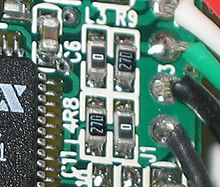
0Ω and 27Ω (27×10
0) surface-mount resistors.
Color-coding of this form is becoming rarer. In newer equipment, most passive components come in surface mount packages. Many of these packages are unlabeled, and those that are labeled normally use alphanumeric codes, not colors.
In one popular marking method, the manufacturer prints 3 digits on components: 2 value digits followed by the power of ten multiplier. Thus the value of a resistor marked
472 is 4,700 Ω, a capacitor marked
104 is 100 nF (10x10
4 pF), and an inductor marked
475 is 4.7 H (4,700,000 µH). This can be confusing; a resistor marked
270 might seem to be a 270 Ω unit, when the value is actually 27 Ω (27×10
0).
A similar method is used to code precision surface mount resistors by
using a 4-digit code which has 3 significant figures and a power of ten
multiplier. Using the same example as above,
4701 would represent a 470x10
1=4700 Ω, 1% resistor. Another way is to use the "kilo-" or "mega-" prefixes in place of the decimal point:
- 1K2 = 1.2 kΩ = 1,200 Ω
- M47 = 0.47 MΩ = 470,000 Ω
- 68R = 68 Ω
For some 1% resistors, a three-digit alphanumeric code is used, which
is not obviously related to the value but can be derived from a table
of 1% values. For instance, a resistor marked
68C is 499(
68) × 100(
C) = 49,900 Ω. In this case the value 499 is the 68th entry of the E96 series of preferred 1% values.
The multiplier letters are as follows:
EIA E96 SMD alphanumeric code
| Letter |
Multiplier |
Decimal |
| Z |
10−3 |
0.001 |
| Y or R |
10−2 |
0.01 |
| X or S |
10−1 |
0.1 |
| A |
100 |
1 |
| B or H |
101 |
10 |
| C |
102 |
100 |
| D |
103 |
1000 |
| E |
104 |
10000 |
| F |
105 |
100000 |
SMT jumpers, marked "0" or "000", are sometimes called "Zero-ohm links" or "0-ohm resistors" although technically they are not resistors.
Transformer wiring color codes
Power transformers
used in North American vacuum-tube equipment often were color-coded to
identify the leads. Black was the primary connection, red secondary for
the B+ (plate voltage), red with a yellow tracer was the center tap
for the B+ full-wave rectifier winding, green or brown was the heater
voltage for all tubes, yellow was the filament voltage for the rectifier
tube (often a different voltage than other tube heaters). Two wires of
each color were provided for each circuit, and phasing was not
identified by the color code.
Audio transformers for vacuum tube equipment were coded blue for the
finishing lead of the primary, red for the B+ lead of the primary, brown
for a primary center tap, green for the finishing lead of the
secondary, black for grid lead of the secondary, and yellow for a tapped
secondary. Each lead had a different color since relative polarity or
phase was more important for these transformers. Intermediate-frequency
tuned transformers were coded blue and red for the primary and green and
black for the secondary.


.jpg)