OLED
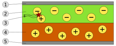
An OLED (organic light-emitting diode) is a light-emitting diode (LED) in which the emissive electroluminescent layer is a film of organic compound
(an organic compound is any member of a large class of gaseous, liquid,
or solid chemical compounds whose molecules contain carbon) which emits
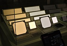
light in response to an electric current. This layer of organic semiconductor is situated between two electrodes. Generally, at least one of these electrodes is transparent. OLEDs are used to create digital displays in devices such as television screens, computer monitors, portable systems such as mobile phones, handheld games consoles and PDAs. A major area of research is the development of white OLED devices for use in solid-state lighting applications.
There are two main families of OLED: those based on small molecules and those employing polymers. Adding mobile ions to an OLED creates a light-emitting electrochemical cell or LEC, which has a slightly different mode of operation. OLED displays can use either passive-matrix (PMOLED) or active-matrix addressing schemes. Active-matrix OLEDs (AMOLED) require a thin-film transistor backplane to switch each individual pixel on or off, but allow for higher resolution and larger display sizes.

Originally, the most basic polymer OLEDs consisted of a single organic layer. One example was the first light-emitting device synthesised by J. H. Burroughes et al., which involved a single layer of poly(p-phenylene vinylene). However multilayer OLEDs can be fabricated with two or more layers in order to improve device efficiency. As well as conductive properties, different materials may be chosen to aid charge injection at electrodes by providing a more gradual electronic profile,or block a charge from reaching the opposite electrode and being wasted. Many modern OLEDs incorporate a simple bilayer structure, consisting of a conductive layer and an emissive layer. More recent developments in OLED architecture improves quantum efficiency (up to 19%) by using a graded heterojunction. In the graded heterojunction architecture, the composition of hole and electron-transport materials varies continuously within the emissive layer with a dopant emitter. The graded heterojunction architecture combines the benefits of both conventional architectures by improving charge injection while simultaneously balancing charge transport within the emissive region

During operation, a voltage is applied across the OLED such that the anode is positive with respect to the cathode. Anodes are picked based upon the fact of how good their optical transparency, electrical conductivity, and chemical stability are. A current of electrons flows through the device from cathode to anode, as electrons are injected into the LUMO of the organic layer at the cathode and withdrawn from the HOMO at the anode. This latter process may also be described as the injection of electron holes into the HOMO. Electrostatic forces bring the electrons and the holes towards each other and they recombine forming an exciton, a bound state of the electron and hole. This happens closer to the emissive layer, because in organic semiconductors holes are generally more mobile than electrons. The decay of this excited state results in a relaxation of the energy levels of the electron, accompanied by emission of radiation whose frequency is in the visible region. The frequency of this radiation depends on the band gap of the material, in this case the difference in energy between the HOMO and LUMO.
As electrons and holes are fermions with half integer spin, an exciton may either be in a singlet state or a triplet state depending on how the spins of the electron and hole have been combined. Statistically three triplet excitons will be formed for each singlet exciton. Decay from triplet states (phosphorescence) is spin forbidden, increasing the timescale of the transition and limiting the internal efficiency of fluorescent devices. Phosphorescent organic light-emitting diodes make use of spin–orbit interactions to facilitate intersystem crossing between singlet and triplet states, thus obtaining emission from both singlet and triplet states and improving the internal efficiency.

Indium tin oxide (ITO) is commonly used as the anode material. It is transparent to visible light and has a high work function which promotes injection of holes into the HOMO level of the organic layer. A typical conductive layer may consist of PEDOT:PSS as the HOMO level of this material generally lies between the workfunction of ITO and the HOMO of other commonly used polymers, reducing the energy barriers for hole injection. Metals such as barium and calcium are often used for the cathode as they have low work functions which promote injection of electrons into the LUMO of the organic layer. Such metals are reactive, so they require a capping layer of aluminium to avoid degradation.
Experimental research has proven that the properties of the anode, specifically the anode/hole transport layer (HTL) interface topography plays a major role in the efficiency, performance, and lifetime of organic light emitting diodes. Imperfections in the surface of the anode decrease anode-organic film interface adhesion, increase electrical resistance, and allow for more frequent formation of non-emissive dark spots in the OLED material adversely affecting lifetime. Mechanisms to decrease anode roughness for ITO/glass substrates include the use of thin films and self-assembled monolayers. Also, alternative substrates and anode materials are being considered to increase OLED performance and lifetime. Possible examples include single crystal sapphire substrates treated with gold (Au) film anodes yielding lower work functions, operating voltages, electrical resistance values, and increasing lifetime of OLEDs.
Single carrier devices are typically used to study the kinetics and charge transport mechanisms of an organic material and can be useful when trying to study energy transfer processes. As current through the device is composed of only one type of charge carrier, either electrons or holes, recombination does not occur and no light is emitted. For example, electron only devices can be obtained by replacing ITO with a lower work function metal which increases the energy barrier of hole injection. Similarly, hole only devices can be made by using a cathode made solely of aluminium, resulting in an energy barrier too large for efficient electron injection.


.jpg)


